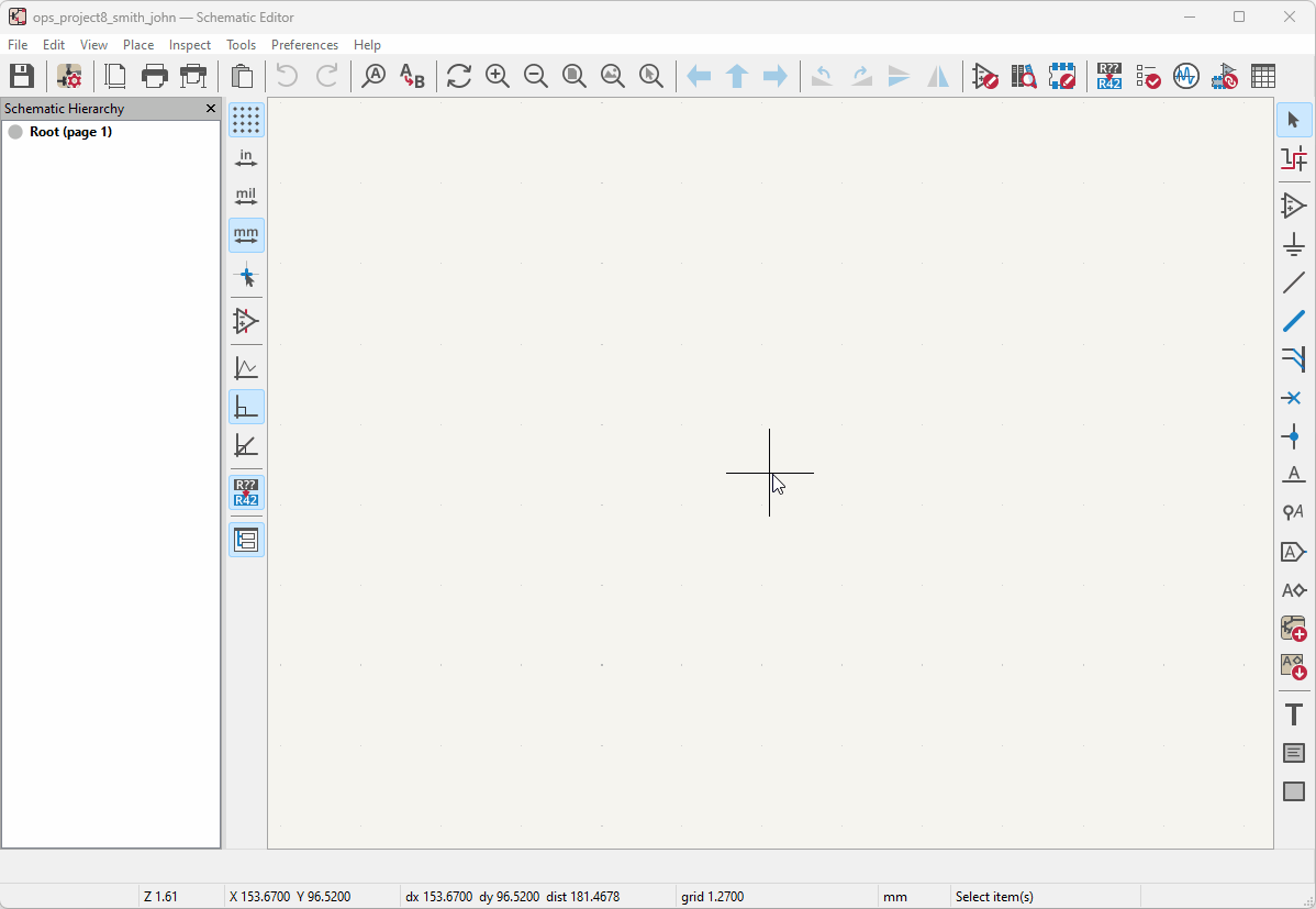
logo
Open Project Space
Projecto · 555 Blinker PCB
PCB design · KiCad · Guided project

Design a complete 555 Blinker PCB with a cleaner, more visual workflow.

This redesigned page keeps the original project structure while improving readability, navigation and visual hierarchy. It also adds a built-in Spanish mode so the page is easier to use in class or in self-study.

Printed circuit board
Updated layout
Better spacing, improved cards and bilingual navigation.
Project overview

From prototyping to a real PCB

Updated 2026.03.14

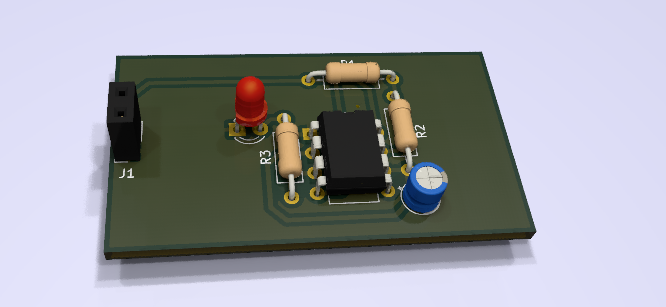
In this project you move beyond breadboards and perfboards and create a complete printed circuit board for the classic 555 blinker using KiCad 7. The objective is to capture the schematic, assign the correct footprints, lay out the PCB and generate manufacturing files.

Recommended setup
  • Use a mouse whenever possible.
  • Save frequently during schematic and layout work.
  • Follow the checkpoints in order.
PCB
Example of PCB board.
Concepts

Printed circuit boards and design workflow

Printed Circuit Boards (PCB)

Printed circuit boards are the standard medium for compact, reliable and reproducible electronic products. They replace temporary prototyping structures with permanent copper traces, pads and footprints connected through a CAD-defined layout.

PCB design overview

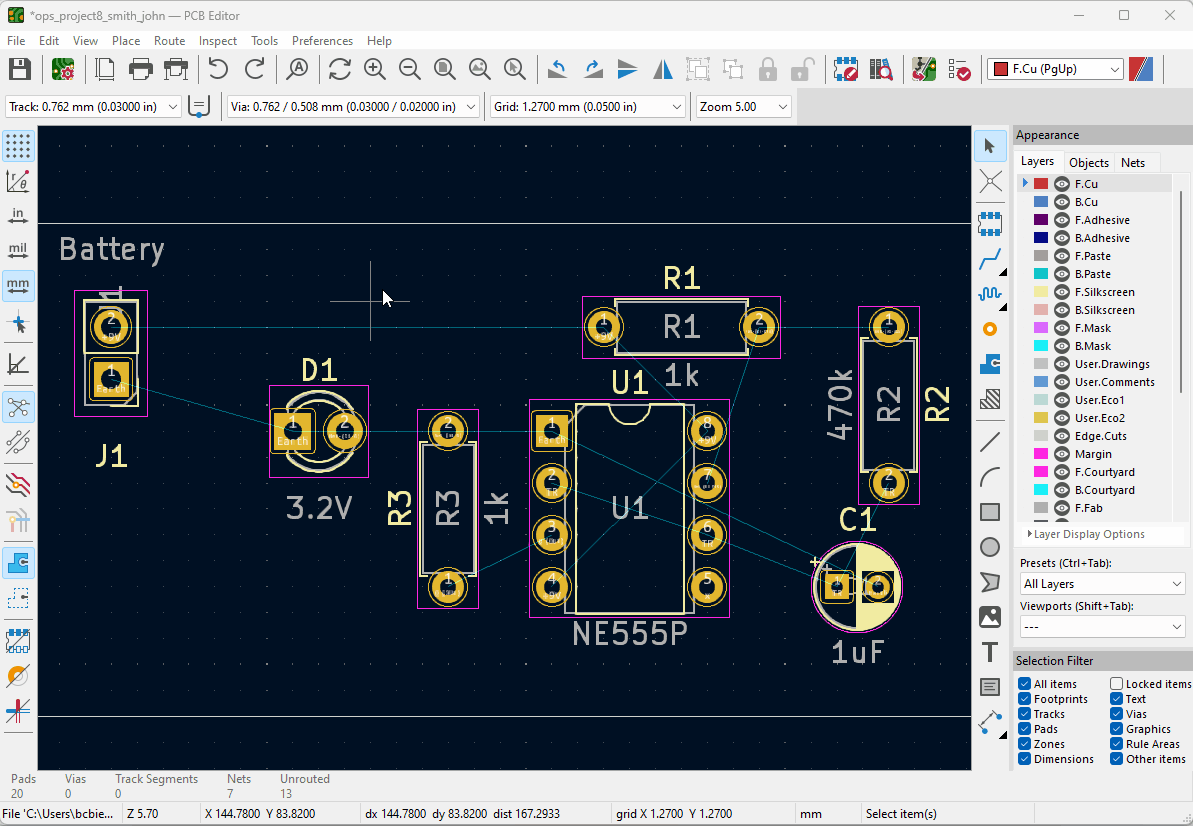
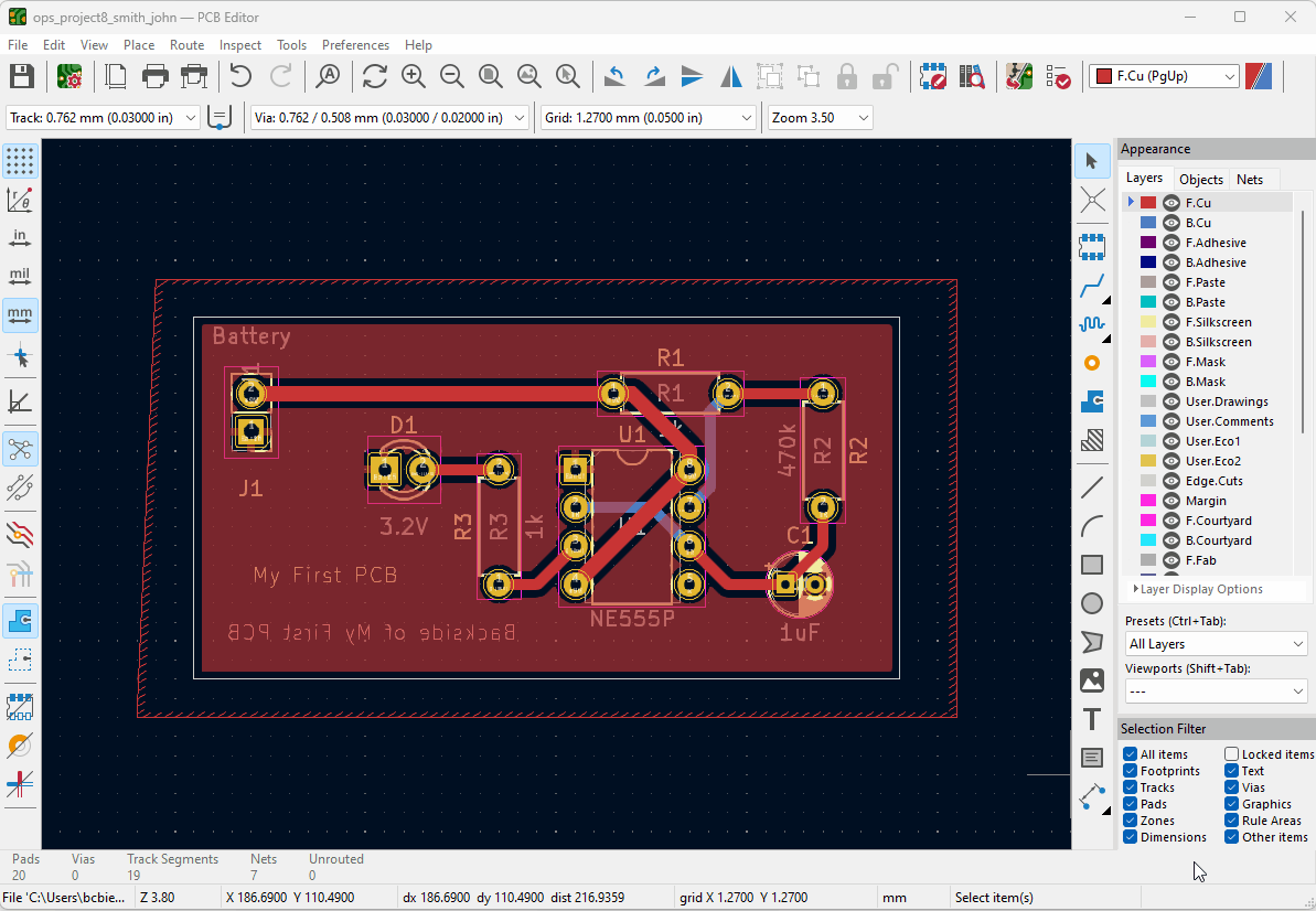
The workflow has two main stages: schematic capture and PCB layout. First, the circuit is translated into a digital schematic with symbols, nets and footprints. Then the board outline is defined, footprints are placed, tracks are routed and manufacturing outputs are generated.

Software setup

Installing KiCad 7.0.11

Use KiCad 7.0.11 for this project. Download the installer for your operating system and keep the default installation settings except for optional help files if needed.

Operating systemDownload
WindowsDownload installer
MacDownload installer
Assessment

Minimum requirements

  • Create a full schematic that reproduces the provided 555 blinker circuit.
  • Pass ERC except for the expected power warning.
  • Create a PCB layout that passes DRC.
  • Use the symbols and footprints listed in the parts section.
Components

Parts and reference selections

This is a compact version prepared for GitHub Pages. Adapt the exact values and footprints to your course requirements.

QtyPartSymbol / valueSuggested footprint
1Timer ICNE555DIP-8_W7.62mm
1LEDD1LED_D5.0mm
2ResistorR1, R2Axial_DIN0207
2CapacitorC1, C2Radial / Disc_THT
1Battery / supply connectorBT1 or J1TerminalBlock / BatteryHolder
Reference diagram

Schematics

Schematic
Reference schematic used to build the PCB.

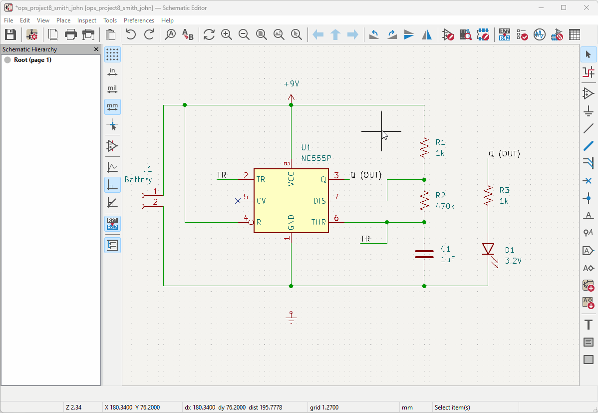
Use the schematic as the basis for your KiCad capture. Check pin orientation, reference designators, values and power connections before assigning footprints and moving to layout.

Tip: keep symbol values and footprint names consistent from the beginning to reduce ERC and PCB update issues later.
Schematic
Example of the PCB.
Step-by-step

Instructions and checkpoints

Follow the checkpoints below in order. Each card is larger than before so screenshots and animated guidance are easier to view on GitHub Pages.

Checkpoint 1

Create the project and capture the schematic

  1. Create a new KiCad project and open the schematic editor.
  2. Add power symbols, parts, values and footprint assignments.
  3. Wire the circuit, add net labels and no-connection flags.
Checkpoint 1
Checkpoint 2

Annotate and validate the schematic

  1. Run schematic annotation to replace placeholder references.
  2. Run ERC and verify that only the expected power warning remains.
Checkpoint 2
Checkpoint 3

Create the board and route the PCB

  1. Open PCB Editor and update the board from the schematic.
  2. Set track and via sizes, define board outline and place footprints.
  3. Route tracks, add vias if needed, and create the ground fill.
Use 40 mil for power/ground and 30 mil for signal traces. Avoid 90° corners.
Checkpoint 3
Checkpoint 4

Run design rule checks

  1. Open DRC and run the checker.
  2. Resolve all violations before generating outputs.
Checkpoint 4
Checkpoint 5

Generate manufacturing files

  1. Plot the fabrication layers and create drill files.
  2. Review the generated files before sharing or submitting them.
  3. Compress the project folder with the required naming format.
Checkpoint 5
Resumen del proyecto

Del prototipado a una PCB real

Actualizado 2026.03.14

En este proyecto pasarás de las breadboards y placas perforadas a una placa de circuito impreso complet del clásico 555 blinker usando KiCad 7. El objetivo es capturar el esquemático, asignar las huellas correctas, diseñar la PCB y generar los ficheros de fabricación.

Configuración recomendada
  • Usa un ratón siempre que sea posible.
  • Guarda con frecuencia durante el esquemático y el layout.
  • Sigue los checkpoints en orden.
PCB
Ejemplo de PCB.
Conceptos

Placas de circuito impreso y flujo de diseño

Placas de circuito impreso (PCB)

Las placas de circuito impreso son el soporte estándar para productos electrónicos compactos, fiables y reproducibles. Sustituyen estructuras temporales de prototipado por pistas de cobre, pads y huellas permanentes definidos mediante CAD.

Visión general del diseño PCB

El flujo de trabajo tiene dos etapas principales: captura esquemática y diseño del layout PCB. Primero se traduce el circuito a un esquemático digital con símbolos, redes y huellas. Después se define el contorno, se colocan las huellas, se enrutan las pistas y se generan los ficheros de fabricación.

Configuración del software

Instalación de KiCad 7.0.11

Usa KiCad 7.0.11 para este proyecto. Descarga el instalador correspondiente a tu sistema operativo y mantén la configuración por defecto salvo opciones auxiliares si las necesitas.

Sistema operativoDescarga
WindowsDescargar instalador
MacDescargar instalador
Evaluación

Requisitos mínimos

  • Crea un esquemático completo que reproduzca el circuito 555 blinker proporcionado.
  • Supera el ERC salvo la advertencia esperada de alimentación.
  • Crea un layout PCB que supere el DRC.
  • Usa los símbolos y huellas indicados en la sección de componentes.
Componentes

Lista de componentes y referencias

Esta es una versión compacta preparada para GitHub Pages. Adapta los valores y huellas exactos según tu asignatura.

Cant.ComponenteSímbolo / valorHuella sugerida
1Circuito integrado temporizadorNE555DIP-8_W7.62mm
1LEDD1LED_D5.0mm
2ResistenciaR1, R2Axial_DIN0207
2CondensadorC1, C2Radial / Disc_THT
1Conector de batería / alimentaciónBT1 o J1TerminalBlock / BatteryHolder
Diagrama de referencia

Esquemas

Esquema
Esquema de referencia usado para construir la PCB.

Usa este esquema como base para la captura en KiCad. Comprueba la orientación de pines, referencias, valores y conexiones de alimentación antes de asignar huellas y pasar al layout.

Consejo: mantén consistentes los valores y los nombres de huellas desde el inicio para reducir problemas de ERC y de actualización hacia PCB.
Schematic
Ejemplo de PCB.
Paso a paso

Instrucciones y checkpoints

Sigue los checkpoints en orden. Cada tarjeta se ha hecho más grande para que las capturas y animaciones se vean mejor en GitHub Pages.

Checkpoint 1

Crear el proyecto y capturar el esquemático

  1. Crea un nuevo proyecto en KiCad y abre el editor esquemático.
  2. Añade símbolos de alimentación, componentes, valores y asignación de huellas.
  3. Cablea el circuito, añade etiquetas de red y marcas de no conexión.
Checkpoint 1
Checkpoint 2

Anotar y validar el esquemático

  1. Ejecuta la anotación del esquema para reemplazar referencias temporales.
  2. Ejecuta el ERC y comprueba que solo queda la advertencia de alimentación esperada.
Checkpoint 2
Checkpoint 3

Crear la placa y enrutar la PCB

  1. Abre PCB Editor y actualiza la placa a partir del esquemático.
  2. Configura tamaños de pistas y vías, define el contorno y coloca las huellas.
  3. Enruta pistas, añade vías si hace falta y crea el plano de tierra.
Usa 40 mil para alimentación/tierra y 30 mil para señal. Evita esquinas de 90°.
Checkpoint 3
Checkpoint 4

Ejecutar las verificaciones de diseño

  1. Abre el DRC y ejecuta la comprobación.
  2. Resuelve todas las violaciones antes de generar resultados.
Checkpoint 4
Checkpoint 5

Generar ficheros de fabricación

  1. Genera las capas de fabricación y los taladros.
  2. Revisa los ficheros generados antes de compartirlos o entregarlos.
  3. Comprime la carpeta del proyecto con el formato de nombre requerido.
Checkpoint 5